Breaking News

Wi-Fi news from Silicon Labs 

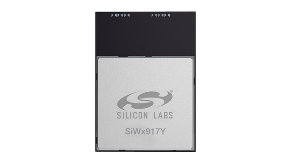
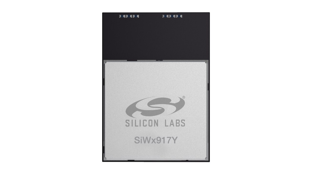
AUSTIN, Texas, Dec. 3, 2024 /PRNewswire/ — Today Silicon Labs (NASDAQ: SLAB), a leader in secure, intelligent wireless technology for a more connected world, announced the SiWx917Y ultra-low power Wi-Fi® 6 and Bluetooth® Low Energy (LE) 5.4 modules.

As an extension of the successful Series 2 platform, these modules are designed to help device makers streamline the complex development and certification process for Wi-Fi 6 devices. The new SiWx917Y modules deliver breakthrough power efficiency while providing robust wireless connectivity, advanced security, and a full-featured application processor, reducing design challenges, product size, costs, and time-to-revenue for device makers. Pre-certified for global regulatory standards and equipped with an optimized antenna, the SiWx917Y modules eliminate the need for lengthy RF optimization and certifications.

“Wi-Fi for IoT has evolved significantly, creating exciting opportunities for innovation. To help end device makers accelerate their full potential, we developed the SiWx917Y Wi-Fi 6 modules,” announced Irvind Ghai, Vice President of Wi-Fi Solutions at Silicon Labs. “These pre-certified modules offer a streamlined solution, enabling manufacturers to easily integrate cutting-edge connectivity into their devices and focus on actual solution differentiation while reducing development costs.”

The modules are ideal for low-power Wi-Fi applications across industries, including smart homes, building automation, healthcare devices, industrial sensors, and asset tracking.

Versatile and Efficient SiWx917Y Modules Deliver Cutting-Edge Wireless Capabilities

The SiWx917Y modules integrate Wi-Fi 6, Bluetooth LE 5.4, an ARM Cortex-M4 application processor, a wireless network processor, large memory, and a rich set of peripherals in a compact 16 x 21 x 2.3 mm package. Key features include:

  • Ultra-low power Wi-Fi 6 connectivity with intelligent power management
  • Dual-core architecture with dedicated application and wireless processors
  • Support for Matter protocol over Wi-Fi
  • Integrated antenna, RF pin and worldwide RF certifications
  • Multiple configurations and operational for design flexibility

The modules’ intelligent power management enables connected sleep mode with as low as 20μA current with Target Wake Time (TWT) and 60-second keep-alive interval. This allows IoT devices like smart locks, thermostats, smart cameras, video doorbells, and industrial sensors to achieve multi-year battery life. The integrated ARM Cortex-M4 processor, large memory, and peripherals also enable sophisticated edge processing capabilities.

The module supports two operational modes: SiWG917Y for SoC (Wireless MCU) mode so customers can execute all application code in the Module’s ARM Cortex-M4 core, and SiWN917Y for NCP mode (Network Co-processor) so customers can execute their application on a separate MCU while the Wi-Fi module manages communication functions.

Meeting the Growing Demands for IoT Connectivity

The explosive growth of IoT devices is driving the need for more efficient and secure Wi-Fi solutions. With Wi-Fi-enabled low-power IoT applications increasing by up to one billion units annually, device makers face the challenge of integrating robust connectivity while addressing concerns about energy efficiency, security, and ease of development.

Availability

The SiWx917Y modules are now generally available for purchase. For more information on Silicon Labs’ SiWG917Y and SiWN917Y Wi-Fi 6 and Bluetooth LE modules, click here.

About Silicon Labs
Silicon Labs is a trailblazer in wireless connectivity for the Internet of Things. Its integrated hardware and software platform, intuitive development tools, and unmatched ecosystem support make Silicon Labs the ideal long-term partner in building advanced industrial, commercial, and home and life applications. Silicon Labs leads the industry in high performance, low power, and security with support for the broadest set of multi-protocol solutions.

SOURCE Silicon Labs

Ask any IoT product developer how much memory their next design will need, and the answer will likely be, more is more! Unfortunately, tiny IoT footprints and constrained hardware resources do not often meet growing memory requirements. This blog describes how much memory IoT devices actually need, and how our SiWx917M Wi-Fi 6 SoCs respond to the IoT developers’ call for more memory.

Despite their small sizes, IoT devices are equipped to run increasingly advanced applications in smart homes, buildings, hospitals, enterprises, and other smart areas of our modern societies. They can run multiple wireless protocol stacks such as Wi-Fi and Bluetooth Low Energy (LE). IoT devices can be connected to several ecosystems through the Matter application layer. Many types of IoT devices can operate autonomously for years in the field. During their operational lifetime, manufacturers push frequent over-the-air (OTA) software updates and security patches to keep their devices current and safe from cyber threats.

IoT Memory Challenge

The challenge for IoT device makers is how to enable all the necessary functions, including the wireless stacks and a complex application on constrained hardware resources, while also accommodating space for OTA updates and future code growth. Memory has become a critical bottleneck for IoT device makers. It’s scarce hardware real estate. However, a large memory enables manufacturers to build better devices with more features and longer lifetime, and it also increases the total value and lifetime of their circuit designs.

This blog explains the IoT memory challenge for non-tech readers: how much memory do you need in an IoT device? How does the SiWx917M Wi-Fi 6 and Bluetooth LE SoC solve the memory challenge with its large memory configuration?

How Much Memory do IoT Devices Need?

IoT devices need memory for a couple of purposes:

  • Wireless stacks: the protocol stacks such as Wi-Fi, Bluetooth LE, and Matter are fairly compact software components, yet they can occupy several hundreds of kilobytes of RAM and a few megabytes of Flash.
  • Customer application: similarly, the (customer’s) device application, whether a smart lock, temperature sensor, or light switch, can occupy hundreds of kilobytes of RAM and megabytes of Flash, depending on the complexity and the amount of data.
  • Software updates: to ensure a fluent and quick execution of OTA software updates, ample space on the Flash must be reserved.
  • Future code growth: software tends to grow over the lifetime of the device and manufacturers need to reserve room on the Flash for future code growth.

The Large Memory Configuration of the SiWx917M

The SiWx917M Wi-Fi 6 SoC features the largest memory configuration in the ultra-low-power Wi-Fi segment. But how much memory do you get with the SiWx917M SoCs, and what can you do with it? Continue reading for a quick description of the SiWx917M SoC memory configuration.

SiWx917M RAM Memory

The SiWx917M SoC features a large internal SRAM (static-RAM) memory of up to 672kB, providing you with more space to execute your application, a security engine, peripherals, Wi-Fi, Bluetooth LE, and Matter protocol stacks. There are three software-configurable memory options for sharing the SRAM between Silicon Labs’ wireless system and your application, allowing you to optimize SiWx917M for various use cases.

SiWx917M In-package Flash

With SiWx917M, you should not run out of flash memory. It provides you with up to 8MB of flash in several alternative configurations depending on the order part number (OPN) (please go to the SiWx917 web page for details).

The large 8MB flash is required in many IoT devices to accommodate the wireless stacks, Matter protocol software, Master Boot Records, bootloader, certificates, OTA software updates, and future code growth.

With the large Flash of SiWx917M, you can develop better, and more advanced IoT devices. It also enables a single-chip architecture, where SiWx917M in SoC operational mode, runs the entire wireless system and your application, reducing device footprint, saving your total BoM and design costs. The large flash allows a longer operational lifetime for your device.

SiWx917M In-package PSRAM

In some cases, IoT software design may need more RAM memory than the 672kB that is available in SiWx917M. Luckily, SiWx917M supports pseudo-SRAM, expanding your execution space radically. The product family includes OPNs, which are equipped with up to 8MB of PSRAM instead of flash.

Note, if both Fash and PSRAM are needed, you can order our SiWx917Y modules, where you can find an OPN with both memory types.

SiWx917M External Flash and PSRAM Expansion

Should you need even more memory than the 8MB flash or PSRAM, SiWx917M supports an encrypted interface to an external flash or PSRAM of up to 16MB, offering ultimate design flexibility and space.

We are convinced that with the ultra-low-power SiWx917M Wi-Fi 6 and Bluetooth LE SoCs, you will have ample memory to accommodate all the functionalities of an advanced wireless IoT device, and you can still allocate space for Matter, OTA updates, and future code growth for the entire lifetime of your device! Go to SiWx917M.

Learn more about the technical details, features, and architecture of the SiWx917M memory.

New Custom Part Manufacturing Service (CPMS) and Device Attestation Certificates (DAC) Injection Streamline Security Implementation for Matter-Certified IoT Devices

AUSTIN, Texas, Oct. 9, 2024 /PRNewswire/ — Silicon Labs (NASDAQ: SLAB), a leader in secure, intelligent wireless technology, in partnership with Kudelski IoT, a division of the Kudelski Group (SIX: KUD.S) and a global leader in digital security and IoT solutions, today announced a new solution to accelerate the time to market for Matter-certified IoT devices. The collaboration integrates Kudelski IoT’s Matter Device Attestation Certificates (DAC) into Silicon Labs’ Custom Part Manufacturing Service (CPMS), enabling device makers to build Zero Trust security from the foundry to customers’ doorsteps, which ultimately saves time and costs.

The Zero Trust approach, with its “never trust, always verify” principle and continuous authentication, is fundamental to Matter, a unifying, IP-based connectivity protocol. Matter mandates unique device authentication certificates using Public Key Infrastructure (PKI) for robust security. While this framework significantly enhances IoT device protection, it also introduces new complexities for manufacturers, particularly in securely obtaining and transferring certificates from Certificate Authorities to production facilities.

By combining Silicon Labs’ secure, economical, and trusted manufacturing capabilities with Kudelski’s certified Matter PKI service, IoT manufacturers can now have Matter DACs securely injected during production, streamlining the path to Matter volume manufacturing.

“The Matter volume production doesn’t have to be a complex hurdle,” said Rohit Ravichandran, product manager for security and services at Silicon Labs. “Our first-of-its-kind secure provisioning service, along with Kudelski IoT’s expertise and PKI services, will enable manufacturers to focus on innovation without compromising on security.”

The integrated CPMS and DAC injection service provides several key benefits:

  • Secure injection of signed DACs at Silicon Labs-designated factories
  • Simplified key management and reduced manufacturing complexity
  • Accelerated time-to-market for Matter-certified products
  • Enhanced protection against counterfeiting and overproduction

“Kudelski IoT’s Matter Product Attestation Certificate Service does the heavy lifting for you, allowing you to join the Matter ecosystem easily,” said Chrystophe Clément, principal architect at Kudelski IoT. “We’re excited to partner with Silicon Labs to scale Matter adoption and reduce the burdens for manufacturers.”

Silicon Labs Matter DAC injection is available now for Silicon Labs’ MG24 wireless SoCs and modules with Secure Vault technology. After completing product development and obtaining Matter certification through the Connectivity Standards Alliance (CSA), manufacturers can easily place orders through the Silicon Labs CPMS web portal. Silicon Labs will then ship sample parts within 4-6 weeks for testing and validation, after which volume orders can be placed.

Learn more about Silicon Labs’ CPMS for Matter devices here.

About Silicon Labs
Silicon Labs (NASDAQ: SLAB) is a leader in secure, intelligent wireless technology for a more connected world. Our integrated hardware and software platform, intuitive development tools, unmatched ecosystem and robust support make us the ideal long-term partner in building advanced industrial, commercial, home and life applications. We make it easy for developers to solve complex wireless challenges throughout the product lifecycle and get to market quickly with innovative solutions that transform industries, grow economies and improve lives. Silabs.com

About Kudelski IoT
Kudelski IoT is the Internet of Things division of Kudelski Group and provides end-to-end IoT solutions, IoT product design, and full-lifecycle services to IoT device manufacturers, ecosystem creators, and end-user companies. These solutions and services leverage the group’s 30+ years of innovation in digital business model creation; hardware, software and ecosystem design and testing; state-of-the-art security lifecycle management technologies and services and managed operation of complex systems. For more information about Kudelski IoT, please visit www.kudelski-iot.com.


SOURCE Silicon Labs

AUSTIN, Texas, Oct. 8, 2024 /PRNewswire/ — Silicon Labs, a leader in secure, intelligent wireless technology for a more connected world, delivered the opening keynote for the inaugural embedded world North America today, with CEO Matt Johnson and CTO Daniel Cooley discussing how AI is driving a revolution in IoT, while detailing the continued success of the company’s growing Series 2 platform and upcoming Series 3 platform.

“AI is rapidly becoming a key growth catalyst that will enable the number of IoT devices to reach over a 100 billion in the next decade,” said Silicon Labs President & CEO Matt Johnson. “Our upcoming Series 3 platform’s unparalleled capabilities and productivity will unlock new applications and new capabilities across a vast range of industries, from manufacturing and retail to transportation, healthcare, energy distribution, fitness, and agriculture, helping transform each sector in remarkable ways.”

To realize this vision, IoT devices need to bring powerful upgrades in connectivity, compute, security, and AI/ML capabilities. Silicon Labs today revealed more information on the Series 3 platform that will make that a reality.

Series 3 SoCs Will Feature World’s Most Nimble Modem, Most Secure and Scalable Memory

Series 3 devices will be able to answer the challenges that the continued acceleration of IoT poses: demands for more processing power at far-edge devices across all IoT applications in key areas including, but not limited to, smart cities and civil infrastructure, commercial buildings, retail and warehouses, smart factories and Industry 4.0, smart homes, connected health, and the demand for increasingly portable, secure, compute-intensive applications. They do this by addressing the key needs of the growing IoT:

  • Connectivity: The full Series 3 portfolio will include dozens of products covering all major protocols and frequency bands, to connect just about anything. The first Series 3 device is designed to include the world’s most flexible IoT modem, capable of true concurrency on three wireless networks with micro-second channel switching.
  • Compute: Series 3 devices will be multicore, with Arm Cortex-M application processors and dedicated co-processors for the radio and security subsystems as well as dedicated high performance machine learning subsystems for select devices. With the most scalable memory architecture in its class, combined with Cortex-M processors ranging from a Cortex-M33 at 133 MHz to dual Cortex-M55s running over 200 MHz, Series 3 devices enable complex applications and embedded real-time operating systems.
  • Security: All Series 3 devices will support Silicon Labs Secure Vault High, with additional features like Authenticated Execute in Place to allow trusted communication between the device and the cloud. Series 3 will also have the world’s most secure memory interface, hardening one of the primary vectors of attack when intruders gain physical access and protecting the device maker’s IP. Series 3 will also incorporate the National Institute of Standards and Technology’s recently released post-Quantum encryption standards.
  • Smart: Select Series 3 devices will feature Silicon Labs’ second-generation Matrix Vector Processor, which offloads complex ML operations off of the main CPU onto a specialized accelerator designed to increase ML performance by up to 100x in wireless, battery-powered devices, drastically reducing power draw.

A key driver in the design for this IoT revolution is data, which flows between edge devices to the cloud and back again. This two-directional flow makes IoT edge devices an ideal partner in the growing world of AI. Not only can the devices be used to make limited decisions at the edge, like smart thermostats that assess ambient temperatures and adjust a home’s HVAC, but also with the advent of massive cloud-based AI applications, edge devices can also play a critical role as data collectors and apply their ML abilities to filter the valuable data from the chaff better. The ability to identify and transmit the data for the “corner cases” that AI operators value to make their systems more intelligent.

The first Series 3 SoC is currently being sampled by customers, and more information will be revealed in the first half of 2025.

Series 1 and Series 2 SoCs Continue to Break the Air Gap

Silicon Labs Series 1 and Series 2 devices continue to be successful in helping to scale the IoT, provide secure, robust connectivity, and open up new applications. The Silicon Labs Series 2 platform grows today with the general availability of a family of new Wi-Fi 6 and Bluetooth LE ICs: the SiWG917 wireless MCU (SoC), the SiWN917 network-co-processor for hosted applications, and the SiWT917 radio co-processor IC targeted for applications running higher end operating systems.  The SiWx917 family is designed from the ground-up for ultra-low-power Wi-Fi 6 applications, offering up to 2 years battery life on a single AAA battery in select IoT applications.

Earlier this year, Silicon Labs announced the BG26 and MG26 devices for Bluetooth and 802.15.4 connectivity. These wireless SoCs are built to be future proof as the needs of the IoT grow and feature the same Matrix Vector Processor for dedicated machine learning as the upcoming Series 3. The MG26 and BG26 doubled their predecessor’s Flash, RAM, and GPIO, and this innovation earned them one of IoT Evolution’s Product of the Year awards.

Silicon Labs Series 2 devices also serve an emerging area around Ambient IoT. This exciting new technology allows IoT devices to draw power from ambient sources in their environment, like indoor or outdoor ambient light, ambient radio waves, and kinetic motion. In partnership with PMIC manufacturer e-peas, Silicon Labs announced the xG22E, a new ultra-low power variant of the xG22 wireless SoC that has a substantially reduced power budget and advanced sleep/wake engines that allow it to operate within the ambient IoT power envelope. This broadly applies to sensors, switches, and commercial applications like electronic shelf labels.

There is still more to come for Series 2 in 2025 and Series 1, Series 2, and Series 3 will co-exist as strong offerings for vast amount of IoT applications.

Learn More About the Future of IoT at the Silicon Labs Works With Developers Conference

These SoCs are just a few members of the broadest portfolio of wireless SoCs and MCUs designed for the IoT. There is no other IoT vendor that matches the breadth, depth, and expertise of Silicon Labs.

To convey that expertise to IoT developers and designers, Silicon Labs is hosting its fifth annual Works With Virtual Developers Conference on November 20 and 21. Free to attend, Works With is the premier developer event for the IoT with over 30 sessions, keynotes, and labs, they can hear about the trends shaping the IoT from experts at Silicon Labs and other industry leaders.

Register for Works With 2024 Virtual and begin building an agenda today.

About Silicon Labs 
Silicon Labs is a trailblazer in wireless connectivity for the Internet of Things. Its integrated hardware and software platform, intuitive development tools, and unmatched ecosystem support make Silicon Labs the ideal long-term partner in building advanced industrial, commercial, and home and life applications. Silicon Labs leads the industry in high performance, low power, and security with support for the broadest set of multi-protocol solutions.

The Smart City Living Lab Wi-SUN Challenge is a dynamic platform that aims to support hardware innovators, start-ups, and academic institutions in developing workable prototypes utilizing the Wi-SUN RF mesh. The challenge encourages them all to harness the potential of the Wi-SUN network. By doing so, they contribute to smarter cities, efficient utilities, and innovative healthcare solutions. With over three hundred members across forty-six countries, the Wi-SUN Alliance drives interoperability and standardization in IoT applications. This challenge aligns with this greater vision.

The thematic areas eligible for the scheme covered domains such as smart cities, energy, water utilities, healthcare, smart parking, metering, smart streetlighting, and more. Focus areas included edge intelligence, predictive maintenance, battery-powered smart utility solutions, etc. We received an overwhelming number of submissions, a total of 266 which consisted of a diverse pool – students, researchers, working professionals, entrepreneurs, and startups—all eager to tackle real-world problems using Wi-SUN technologies. All the teams provided not only their ideas but also detailed plans for executing their projects including budgetary and component requirements.

A thorough screening process was undertaken by our esteemed judge panel – Dr. Aftab Hussain, Mrs. Anuradha Vattem – Lead Architect from IIITH, Venkatesh Narasimhan, and Srinivasa Dukkipati from Silicon Labs, which took place in three stages, the first based on the relevance to the smart city applications, the second based on their understanding on sensors and cloud connectivity, and the final round, which was an online interview round designed to check their capability to ready their concept in the stipulated amount of time, their experience with IoT applications and their understanding on Wi-SUN.

Our expert panel narrowed down the submissions, after thorough review and discussions and announced the chosen Top 10. Consisting of six teams from startups and four from college students, the ideas were innovative and fresh. These finalists, spanning four Indian States, are poised to make a difference with their ideas. Ranging from smart dustbins, particulate matter monitoring devices, and real-time water quality monitoring systems to warehouse management bots and real-time soil monitoring, they have it all covered.

In the first week of August, a one-day workshop will have been planned for the ten finalists to give them hands-on experience with the LFN (Limited Function Node) HW kit and SW development platform, following which the participants will begin the development of the application.

Once the concepts are built, in the final leg of their journey, the ten teams will evaluate the PoC at the Living lab using the existing Wi-SUN backbone network in the IIIT Hyderabad campus.

The winners would then be finalized by the panel of experts followed by the award ceremony where the winners will take home grand cash prizes worth Rs. 8 lakhs (9.6 k in USD).

The Wi-SUN Challenge is a collaborative effort between IIITH Smart City Living Lab and Silicon Labs, as part of their campus-wide Wi-SUN network initiative. The Wi-SUN Challenge has been a tremendous success so far. However, this is not just a competition—it is a catalyst for real-world impact. It is about working together and striving to make substantial changes in the world around us.

Broadband internet subscriptions once seemed like a forever-growing cash generator for service providers. Unfortunately, the growth has plateaued in most developed markets, and the leading ISPs and telcos are now integrating new IoT capabilities on their Wi-Fi gateways in anticipation of the Smart Home transformation. However, simply putting a Thread 802.15.4 wireless chip in a CPE and rolling it out to millions of subscribers is not yet enough for a viable smart home business. In this blog, Christopher Ince from Silicon Labs explains seven aspects of IoT that ISP and telco leaders should consider in order to build a stickier smart home business.

Smart home vision

The Broadband Plateau

In just two decades, the number of global fixed broadband connections increased nearly eight-fold from 200 million to 1.5 billion. This historical growth era, which really took off at the advent of the millennium, has churned fortunes for internet service providers (ISPs) and telcos worldwide. Great cash cow, you might think. Well, it had its moment. Today, the fixed broadband markets in most developed countries have saturated, according to the OECD Broadband Portal. This has led to intense competition, increasing customer acquisition costs, price erosion, and churn, hitting the service providers’ bottom lines. In the USA alone, nearly 3,000 broadband ISPs are fighting for the dollars Americans pay every month to get the information highway flowing into their homes.


Smart Home Benefits to Internet Service Providers (ISPs)

The global ISP market was valued at USD 390 billion in 2022 and is projected to reach USD 566 billion by 2032, expanding at a CAGR of 3.9% during this period. Despite promising industry forecasts, the old broadband growth strategies do not apply anymore, and service providers need new ways to grow business.

Bundling new smart home services and IoT connectivity technologies into broadband subscriptions has quickly become one of the most promising ways for the leading ISPs and tTelcos to accelerate their business.

Smart home and IoT provide many clear benefits to service providers – they can become the complete provider of wireless IoT home connectivity alongside Wi-Fi, managing and optimizing connectivity for all types of IoT devices used in homes today and in the future. Owning the home IoT infrastructure, e.g., OpenThread Border Router (OTBR) capability, allows service providers to claim a strategic position in the greater smart home ecosystem and do meaningful and sustained business alongside global smart home brands such as Amazon, Apple, Google, and Samsung. Smart Home and IoT services also help service providers enable new revenue sources, improve customer value-add, and strengthen customer retention, thus improving subscription business and reducing churn.

Facts isp and telecom leaders should know about iot fig1

Figure 1 Internet Service Providers are transforming their legacy Wi-Fi CPE base into a multi-protocol IoT home infrastructure by adding Thread 802.15.4 and other low-power wireless protocols to complement Wi-Fi.

Seven IoT Aspects ISP and Telco Leaders Should Consider

We are witnessing a trend of ISPs and telcos recognizing that it is their role to own the wireless IoT infrastructure of connected smart homes. However, simply integrating a Thread 802.15.4 wireless chip inside Wi-Fi home gateways and rolling them out to millions of subscribers is not yet enough. There are seven critical aspects of IoT that ISP and telecom leaders should consider before locking their smart home strategies:

  1. IoT Infrastructure – The existing legacy CPEs typically support Wi-Fi connectivity only. However, the smart home IoT device market is proliferating rapidly, and Wi-Fi is not optimal for all device types. In fact, many emerging IoT devices will use a more energy-efficient and lightweight mesh connectivity technology such as Thread. So, building a scalable and future-proof IoT home infrastructure that supports Wi-Fi, Thread, and even other wireless IoT connectivity technologies such as Bluetooth Low Energy (LE), is the first step service providers should consider. How to choose the right set of IoT technologies that allow you to cover all home IoT connectivity needs today and in the future? Silicon Labs has years of experience in helping service providers and gateway manufacturers to enable optimized wireless multi-protocol IoT solutions such as OpenThread Border Router (OTBR) on gateways.
  2. Matter Gateway – As described earlier, enabling wireless IoT infrastructure is the first step toward a scalable and future-proof smart home business. However, if you want to enhance your business from a mere IoT connectivity provider to offering value-added smart home applications to your customers, Silicon Labs’ multiprotocol wireless SoCs, MG21 and MG24, enable the Matter Gateway capability on your CPE, allowing you to increase revenue through your own, branded Matter ecosystem, bundle devices of any manufacturer via the Matter protocol, and allow users to control them all via your App, Amazon, Apple, Google, and, Samsung.
  3. Wireless Performance – Every home imposes a unique combination of wireless challenges to service providers – concrete walls, metal surfaces, windows, and other sources of interference can deteriorate user experience, burden your customer service centers, and increase operational costs. As a service provider, you must optimize IoT wireless performance on your gateways to enhance user experience, regardless of where the gateway sits in any given home environment. Silicon Labs IoT solutions are renowned for their superior wireless performance – such as the MG24 multi-protocol chip that offers the market-leading link budget and antenna diversity, delivering efficient connectivity in every corner of the home and beyond.
  4. Wi-Fi Co-existence – With the legacy Wi-Fi-only home gateways, service providers didn’t have to worry about 2.4 GHz multi-radio/multi-protocol interference. However, with smart home gateways combining Wi-Fi and IoT radios such as Thread, you will face a new challenge: how to manage Wi-Fi co-existence? Silicon Labs can help you to design the most effective Wi-Fi co-existence solution on your gateway using, e.g., our advanced Packet Transmission Arbitration (PTA) and the patent-pending Signal Identifier capabilities.
  5. Energy Consumption – Energy regulations such as the new, stricter EU Ecodesign Standby Regulation 2023/826 (HiNA) effective 2027, will limit the standby power consumption of consumer CPE down to ≤7W, forcing service providers to reduce the gateway power consumption radically. Silicon Labs provides you with many innovations for more energy-efficient gateway design – for example, you can allow users or network operators to turn the power-hungry Wi-Fi transceiver off and on remotely during nights, weekends, or vacations using our patent pending Thread solution, or Bluetooth LE.
  6. Platform Integration – Building an IoT infrastructure that scales to millions of homes and supports new devices, services, and connectivity technologies for years to come requires seamless integration of dozens of building blocks. Managing them can become an integration nightmare. To make things easier for service providers, Silicon Labs offers an end-to-end one-stop-shop solution for building a scalable and future-proof IoT home infrastructure. This includes high-performance and ultra-low-power multiprotocol wireless processors, pre-verified wireless software stacks, tools, security, always up-to-date Matter implementation, online Matter Developer Journey, and a Connectivity Lab where you can test your gateways and devices in a friendly environment before taking the official certification tests.
  7. Interoperability – A smart home solution without seamless interoperability between gateways, devices, protocols, and ecosystems is like a symphony orchestra without a conductor. If the devices are not playing the same tune, the user experience suffers, customers are frustrated, and vote with their feet. Silicon Labs has worked for decades to become the conductor of the smart home industry – we provide tested and verified wireless IoT and Matter solutions to both, gateway and device makers, allowing us to perfect our standards compliancy and system interoperability, ensuring that you can build a smart home experience where every component plays the same tune.

As companies strive to create greener and more ecologically conscious products and device ecosystems, the world of IoT is constantly adapting to embrace this shift. From smart home devices like locks and sensors, to industrial devices like factory monitoring equipment and machinery sensors, battery-less and low-power-consuming solutions are revolutionizing and reshaping the future of sustainable IoT.

The Problem with Batteries

The IoT is all about creating an inter-connected world; where innovative and intelligent devices interact seamlessly with each other to transform how we experience technology in our everyday lives.

However, every device needs to be powered to achieve this level of interconnectivity. While this power can have many sources, the most common and simplest source for IoT devices is a traditional battery.

So, what’s the problem? If traditional batteries are the simplest answer, why are consumers and device makers suddenly striving for a battery-less future?

Well, let’s get into it.

First, batteries are a menace to the environment. Not only is their disposal inconvenient, but improper disposal and recycling practices cause significant harm to ecosystems. Every year, more than 15 billion used batteries find their way to landfills. They contain acid and toxic metals like lead and mercury, which leads to the release of about 900,000 tons of hazardous, soil-and-groundwater-polluting waste into the environment.

Second, batteries have a limited lifespan. This requires constant replacing or recharging, which can be costly and time-consuming depending on the type of device, how much power it consumes, and how frequently the battery needs to be replaced or recharged. All of this adds up to the maintenance cost of the device.

Third, as the number of connected devices in a network is expected to grow rapidly, so will the number of batteries. The concept of IoT connectivity benefits relying on batteries threatens their adoption and scalability.

Ambient IoT – A New Class of Connected Devices

To address the challenges and drawbacks that batteries impose on smart connected devices, pioneers in IoT are now navigating their way into a new, energy-aware, battery-less future of connected devices. This realm of IoT, collectively referred to as Ambient IoT, aspires to achieve seamless connectivity without the environmental and functional implications that come with it.

What is Ambient IoT?

Ambient IoT refers to the class of connected IoT devices that harvest naturally available energy sources such as magnetic electric fields, light, thermal differential, kinetic energy, and vibration to power them. These sources, also referred to as Ambient sources of energy, can reduce the dependency on — and potentially even replace the need for — batteries, leading to products with flexible form-factors lower BOM costs and vastly longer product lifetimes.

An important term here is harvesting. Ambient IoT and Energy Harvesting are different yet related concepts. Energy Harvesting refers to the process of harnessing, transforming, and then storing energy from various ambient sources like solar power, RF waves, and physical vibration.

Ambient IoT leverages Energy Harvesting technologies to power a new era of devices targeting applications that rely on short-range, wireless connectivity. These applications include smart home devices like switches and locks, smart buildings, asset tracking, smart metering, and factory automation.

However, before we jump to these applications of Ambient IoT, let’s dig deeper into why energy-efficient solutions are not only essential to IoT but can also potential game-changers.

Why Should Designers Embrace Ambient IoT Designs?

With Ambient IoT, our beloved smart devices can now rely on natural sources of energy to draw power and maintain connectivity instead of relying on conventional batteries. These sources (like light, heat, motion, etc.) extend the device’s lifetime and notably reduce the detrimental impact that batteries have on the environment. But how is relying on these sources for power any better than relying on traditional batteries? Why is there a sudden shift to powering devices through renewable sources of energy? Well, there are quite a few reasons:

Enables a Greener Future for Customers
Not relying on batteries- or reducing the amount consumed by smart devices- contributes to a healthier ecosystem. As previously mentioned, improper battery recycling or disposal practices contaminate the environment by releasing toxic metals like lead, cadmium, mercury, and lithium.

Improves Scalability
An IoT solution is only as strong as its network size and scale of adoption. Having a denser and more reliable network can potentially increase the range and frequency of communication between devices. For example, communicating with nearby gateways is important in asset tracking to ensure better traceability and reduce the risk of losing valuables. Another example is a smart building and how its energy rating can be improved if more sensors are deployed. If each of these sensors requires a battery cost and replacement, the benefits at scale are diminished. Integrating battery-less nodes into the network can help mitigate this problem. Additionally, the constant need for battery replacements increases demand, and when the supply cannot keep up with this rising demand, it causes scalability issues.

Helps with Long-Term Cost Savings
Not relying on traditional batteries to power your device can impact the BoM) cost in quite a few ways. On one hand, it may decrease this cost by eliminating the need to constantly replace batteries. On the other hand, it could also increase the BoM cost as energy harvesting components like Integrated power management systems may be more expensive to install than traditional batteries. However, the long-term cost savings from reduced maintenance and extended lifespan of battery-less devices often outweigh the initial increase in the cost of developing these devices.

Additionally, traditional batteries must regularly be replaced or recharged. This maintenance is not only time-consuming but also adds to the overall cost associated with owning and maintaining a smart device. In the US alone, an average household buys over 90 batteries annually, and most of them do not even have a 10-year lifetime.

Fosters Innovation
Battery-less architecture allows for a more compact device by eliminating the need for the previously reserved socket for traditional batteries. This is particularly beneficial for devices like wearables and implanted medical devices where size and weight are essential considerations. This battery-less design also helps create more durable devices, eliminating the risks associated with battery degradation and failure. Additionally, the saved hardware space can also be used to add more peripherals, driving innovations in the boards’ physical design and technical features. This push towards battery-less devices also serves as a catalyst for the development of eco-friendly and sustainable innovations in IoT.

Unlocks New Use Cases
By fostering innovation, Ambient IoT can also unlock new use cases that would not have been convenient to implement with a battery-reliant architecture. For example, in smart agriculture, applications for crop management that are installed in greenhouses are very difficult to replace after installation. They require sensors to be installed all over the field, and having to replace the batteries in these sensors is time-consuming, labor-intensive, and costly. The notion of running wires to power these systems is even more impractical because they are prone to breaking due to the harsh conditions of the application. The abundance of solar power in a greenhouse or the vast amount of vibration created on machinery can easily be harvested to power these sensors.

While all these advantages make a great case for Ambient IoT, relying on natural sources to power smart devices also poses some challenges. An ambient IoT source can only produce limited amounts of power compared to traditional batteries. This makes them more suitable for smart devices that consume low to moderate amounts of power. Furthermore, Ambient IoT is best suited for devices that are designed for a specific function like beaconing, brief periodic advertisement, or intermittent connections to a gateway for data logging status and have low reconfigurability. This is also because of the limited power supply from energy efficient methods. However, these types of devices have the ability to be energy conscious and therefore make energy-awareness based decisions dynamically. For instance, based on available energy, an IoT radio may choose to shorten its payload and interval and instead opt to remain in a deeper sleep mode for longer while it regenerates more energy.

Ambient IoT Applications

With Ambient IoT, developers can now build devices using an energy-friendly platform that minimizes power consumption, improves device longevity, and decreases the device’s reliance on traditional batteries. Many current IoT applications can potentially switch to ambient and power-optimized solutions.

  • Smart Buildings: Kinetic pulse-harvesting battery-less doorknobs and light switch controls using Zigbee Green Power helps decrease the need to constantly replace batteries and render an office building more intelligent by allowing switches to be moved around different spaces without the need for renovation.
  • Asset Tracking: Tracking and managing warehouse inventory is challenging, but asset tags and other tracking systems make it so much easier! However, they need to have their battery replaced quite so often. Ambient IoT provides battery-optimized solution that reduces this reliance on batteries or allows for adoption of battery-less tag design which offer a significant improvement from manual barcode scanning.
  • Agriculture: Sensors are used to help monitor and map greenhouse and vehicle conditions, get real-time information on temperature, humidity, and other environmental factors, as well as monitor cattle and their health in the barn. Battery-less solutions makes the implementation of smart agriculture easier by eliminating the need to constantly replace batteries in sensors that help automate farming.
  • Smart Home and Appliances: Smart home appliances such as door locks, faucets and switches help automate residences and build a smarter, more-connected home. In this use case, battery dependencies and their associated replacement costs can be eliminated by using energy-harvesting design. power harvesting generators.
  • Gaming Electronics: Indoor solar and RF powered television remote controls, and computer keyboards provide an energy-efficient and cost-efficient Bluetooth solution.

Some other key applications include tire pressure monitor sensors (TPMS), ESLs, factory automation, and predictive maintenance machine monitoring using vibration and thermal energy harvesting.

Silicon Labs and Ambient IoT

As we venture into a more connected and intelligent future of smart devices, it is important that leaders in IoT do not fall behind in this shift. It is imperative for experts and companies to invest time and resources into Ambient IoT and other energy-efficient solutions and stay ahead of the curve to meet their ESG goals. This will help us navigate a more sustainable future of IoT and help us strike a balance between technological advancements and environmental sustainability.

At Silicon Labs, it is our mission to enable wirelessly connected devices that transform industries all over the world. Achieving seamless inter-connectivity in an increasingly digital world is our utmost priority. To help ensure the future of IoT is ecologically responsible, we have now optimized our xG22 line of SoCs (BG22E SoC, MG22E SoC, and FG22E SoC) to include features that will support energy harvesting.

With a dual Cortex-M33 and Cortex M0+ radio core, the xG22E is our most energy-friendly SoC to date. It is the ideal choice for developers who are looking to build low-power consuming, high performing smart devices, that function on a battery-optimized, energy-efficient platform. It is the ideal choice for device-makers looking to implement a solution that offers an ultra-fast, low-energy cold start, low-energy deep-sleep wake up, and efficient energy mode transitions that mitigate harmful current spikes and prevent damage to the storage cells.

In addition to our radio board and xG22E Explorer Kit, we are e-peas , an industry leading provider of PMIC, to develop an Explorer Kit Shield. This kit consists of the Explorer Kit and 3 shields that fit onto the Explorer Kit board. The first shield allows for experimentation with alternative battery chemistries and supercapacitors, the second shield is dedicated for kinetic/pulse harvest applications, and the third shield allows developers to experiment with dual harvest sources simultaneously.


In an increasingly connected world, the IoT has become an integral part of our daily lives. From smart home devices to wearable gadgets, IoT devices are making us more productive, healthier, and bringing new levels of convenience. But robust and reliable connectivity is critical. Enter Amazon Sidewalk, a shared wireless network designed to extend the reach of IoT devices beyond the confines of our homes. This not only revolutionizes IoT connectivity but also bridges the gap between neighborhoods.

What Is Amazon Sidewalk?

With the idea of making our world smarter, safer, and more interconnected, Amazon Sidewalk comes as a novel concept that leverages existing Amazon Echo and Ring devices as bridges to create a neighborhood-wide network. It not only revolutionizes IoT connectivity by extending the range of devices but also bridges the gap between homes and neighborhoods.

Here’s how it works:

  • A Shared Network: Amazon Sidewalk allows compatible devices to communicate with each other over a shared network. This network extends beyond individual homes, connecting devices across a broader area.
  • Low-Bandwidth, Long-Range Connectivity: Amazon Sidewalk provides reliable connectivity even at low bandwidths. It’s ideal for devices such as outdoor lights, motion sensors, and location-based trackers.
  • Communication Protocols: Amazon Sidewalk uses multiple communication protocols:
    • Bluetooth Low Energy (LE): For short-distance communication within a home.
    • CSS and FSK Radio Protocols: These operate at 900 MHz frequencies, enabling longer-range communication.

The Architecture of Amazon Sidewalk

Amazon Sidewalk’s architecture consists of three layers:

  • Radio Layer
    • Amazon Sidewalk devices communicate using Bluetooth LE, CSS, or FSK.
    • The application layer sits on top of the Bluetooth LE stack for Bluetooth LE devices.
    • For FSK and CSS, there’s an additional network layer.
  • Network Layer
    • Handles routing and forwarding of data between devices.
    • Ensures seamless communication across the Amazon Sidewalk network.
  • Application Layer
    • Manages device-specific applications and services.
    • All Amazon Sidewalk devices connect to the cloud via AWS IoT Core for Amazon Sidewalk.

Silicon Labs: Enabling Amazon Sidewalk Devices

Silicon Labs, a leading provider of IoT solutions, offers a comprehensive development ecosystem for Amazon Sidewalk devices:

  • Amazon Sidewalk SDK: Our certified SDK simplifies development, reduces costs, and accelerates time-to-market for Amazon Sidewalk devices.
  • Wireless Hardware: Silicon Labs offers a range of hardware options, including the SG28 dual-band SoC, SG23 SoC, and BG21/BG24 Bluetooth LE modules.
  • Security: Security is paramount in IoT, and Silicon Labs ensures robust security features for Amazon Sidewalk devices.
  • Development Kits and Tools: Developers can access integrated tools and services, from concept to product launch.

Collaboration with Amazon

Silicon Labs collaborates closely with Amazon to drive long-term success:

  • Hardware Roadmaps: Continual innovation ensures compatibility with Amazon’s evolving ecosystem.
  • Software Updates: Regular updates enhance device performance and security.

Choose the Right Hardware when Developing Amazon Sidewalk Devices

Silicon Labs’ Amazon Sidewalk Hardware Selector Guide was created to assist developers in selecting the ideal module or SoC and the associated development hardware for their Sidewalk-enabled devices.

The Smart City Living Lab at IIIT Hyderabad plays a pivotal role as a testbed and proof of concept for emerging smart city technologies in the challenging Indian market. In 2022, we delved into the initial Wi-SUN deployment and the subsequent migration from Wi-SUN FAN (Field Area Network) 1.0 to FAN 1.1, emphasizing the significance of each phase. As we transitioned from 2023 to 2024, the focus of the Smart City Living Lab shifted. Rather than solely deploying the infrastructure that forms the backbone of the Wi-SUN network, we began integrating low-power nodes. These nodes allowed us to explore how environmental sensors, water meters, and other battery-powered devices could leverage this infrastructure to enhance intelligence in our surroundings.

Battery-powered sensor nodes have been strategically deployed across the campus. These nodes transmit data to the oneM2M server using a variety of communication infrastructures, including 4G, LoRaWAN and Wi-Fi which follow a point-to-point network.

Wi-SUN FAN operates as a mesh network protocol where each device can directly communicate with its neighboring devices, allowing messages to travel over long distances by hopping between nodes. This robust approach ensures reliable connectivity even in challenging environments. What makes Wi-SUN FAN truly remarkable is its self-forming capability. When new devices are added, the network dynamically adapts and integrates them seamlessly. Furthermore, the network is self-healing, meaning if a communication pathway encounters an obstacle or fails, the system automatically reroutes data to ensure it reaches the designated gateways or central servers. This resilience ensures uninterrupted data flow and enhances the overall efficiency of our smart infrastructure.

Wi-SUN FAN 1.1 introduces a limited function node (LFN) device, also known as a low energy (LE) node. These LFNs are designed with lower power consumption and efficiently support battery-powered equipment. Their remarkable battery life of 15 to 20 years makes them ideal for various applications, including gas and water metering, environmental monitoring, traffic sensing, parking management, and weather sensors. With the integration of LFN nodes into the Wi-SUN mesh network, they now serve as the wireless interface for battery-powered sensors. This seamless communication over the Wi-SUN network ensures data flow to the oneM2M server, enhancing the overall efficiency of the smart infrastructure on the campus.

LFN Architecture

LFNs offer essential capabilities such as PAN (personal area network) discovery/joining and IPv6 packet communication. These LFNs share the same communication stack as full function nodes (FFNs) but with a restricted listening schedule to optimize power consumption and don’t have routing capability. However, LFNs operate exclusively within a PAN rooted at a FAN 1.1 Border Router. They function as children of a FAN 1.1 Router rather than serving as parents to other nodes.

Refer to the diagram below for further clarity:

living-lab-architecture-phase-3

Wi-SUN Impact on Smart Cities

As cities evolve into smarter ecosystems, they strive to enhance the quality of services by closely monitoring infrastructure and environmental factors. Applications such as water and gas consumption tracking, as well as air-quality monitoring, provide real-time information to the public. This data empowers individuals to make sustainable lifestyle adjustments and protect themselves from harmful pollutants.

The Government of India has set an ambitious goal to replace existing meters with more than 250 million smart energy meters by 2025. To achieve this while ensuring reliability and security, a connectivity standard that scales is essential. Wi-SUN, with its resilient and interoperable standards-based Sub-GHz mesh solution, stands out in the realm of smart grid and smart city applications.

Here’s why Wi-SUN stands out:

  1. Scalability: Wi-SUN’s scalability allows it to handle a vast number of devices efficiently. With over 95 million Wi-SUN-capable devices deployed globally, it has proven its unique scalability even in challenging environments.
  2. Reliability: Wi-SUN offers a high level of network reliability. Its mesh topology ensures that even if individual nodes fail, the network remains resilient.
  3. Cost-Effectiveness: Wi-SUN’s low total cost of ownership makes it an attractive choice for large-scale deployments.
  4. Security: Security is a top priority for Wi-SUN FAN. Its native public-key infrastructure (PKI) integration provides certification capabilities for each device. This prevents malicious reprogramming and validates incoming firmware updates, which is crucial for long-term deployments. IPv6 Support: Wi-SUN’s support for IPv6 enables robust networking security features, including intrusion detection, traffic shaping, network analysis, and penetration testing. It outperforms its rivals by maintaining network visibility down to the end devices themselves.

In summary, Wi-SUN FAN plays a pivotal role in shaping smarter cities and ensuring reliable connectivity, security, and efficiency. Smart cities can harness the existing wireless communication infrastructure offered by Advanced Metering Infrastructure (AMI) or street lighting networks to empower a range of adjacent applications. These include smart traffic signals, public transit signs, parking spaces, electric vehicle (EV) charging stations, and more. By leveraging this infrastructure, cities enhance connectivity, efficiency, and sustainability, creating a more intelligent urban environment.

Trade-offs with Cellular Communications

One of the tradeoffs is that cellular systems must be upgraded regularly to keep up with carrier-required updates and sometimes protocol sunsets that require replacing underlying hardware. Most Internet of Things (IoT) devices operate on batteries, making power efficiency crucial. Cellular communications demand relatively high power due to the need to communicate with distant towers (sometimes up to half a kilometer away).

Geographic Coverage vs. Device Density

Choosing between cellular and RF mesh networks depends on network requirements. Cellular connectivity is ideal for extensive geographic areas with sparse network devices. It provides wide coverage but consumes more power. RF Mesh Systems are suited for dense device deployments and offer localized coverage and lower power consumption. While newer IoT cellular protocols offer reduced current draw and sleep modes, they still drain batteries much faster than RF communication modules.

Enhancing Campus Connectivity: LFN Deployment

In the third phase of Wi-SUN mesh network deployment, we introduce LFNs powered by Silicon Labs’ EFR32FG28 SoC. Let’s delve into the details:

The EFR32FG28 SoC is an ideal dual-band Sub-GHz + 2.4 GHz Bluetooth LE SoC. FG28 is a multi-core solution that provides industry-leading security, low power consumption with fast wakeup times, and integrated power amplifiers to enable the next level of secure connectivity for IoT devices. Integrating an AI/ML Hardware Accelerator enables faster, lower-power inferencing for low-power end nodes. During the third phase deployment of LFNs, various sensor devices that were previously out of reach will now be able to connect to the cloud via Wi-SUN Mesh.

Concluding the Wi-SUN Journey: A Thriving Ecosystem

The Living Lab at the IIIT-H campus has successfully cultivated a robust Wi-SUN ecosystem. This dynamic network now plays multiple pivotal roles:

  1. Hackathons and Innovation Challenges:
    • The Wi-SUN mesh network serves as an experimental playground for hackathons, fostering creativity and rapid prototyping.
    • Startups leverage this environment to validate their proof-of-concepts, pushing the boundaries of what’s possible.
  2. Real-World Testing:
    • Network service providers could conduct rigorous field tests within this smart city Living Lab.
    • The Wi-SUN mesh network’s reliability and scalability are put to the test, ensuring its readiness for practical deployment.

The Wi-SUN ecosystem thrives within the IIIT-H campus, bridging theory and practice and propelling us toward a connected future.